
")
6寸绝缘体上碳化硅(SICOI)
上海奥麦达微可以提供4寸和6寸的4H-SICOI晶圆

我们提供 4-6寸的 4H-SICOI晶圆(绝缘体上碳化硅晶圆),该晶圆采用亲水键合或者表面活化键合技术将热氧片和导电型碳化硅晶圆或者高纯半绝缘碳化硅晶圆键合在一起,然后通过离子注入,退火,减薄的方式或者直接减薄和CMP抛光的方式,将厚度控制到您所需要的厚度,值得注意的是离子注入和 直接CMP和减薄这两种方式有各自的优缺点。我们为客户提供多种SICOI产品。
基于SMARTCUT工艺(一般mems领域会用)
膜厚范围:50nm-20um
膜厚均匀性+-20nm
基于Grinding+CMP工艺(量子和光学领域用)
膜厚范围:200nm-任意厚度
膜厚均匀性:+-100nm:
数据支持:
下面是我们的基于两种工艺的一个参考规格书,如果想要了解更多 ,请联系我们
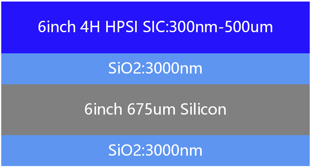
Grinding-CMP fabricated 6 inch SiCOI(膜厚精度+-100nm)
规格书
High-purity semi-insulating 4H-SiC, on-axis, Orientation: {0001} ±0.25 deg, thickness: 1um±0.1um;
SiO2 thickness 3um,Si (100) 675+-25um
SiC C-face up, roughness Rq<0.2nm (5um*5um)after CMP
表面质量数据
Smartcut fabricated 6 inch SiCOI(膜厚精度+-20nm)
High-purity semi-insulating 4H-SiC, on-axis, Orientation: {0001} ±0.25 deg, thickness: 1um±0.02um (Wafer specification need to be checked before processing)
SiO2 thickness 3um
Si (100)
SiC c-face up, roughness Rq<0.2nm after CMP
离子注入可以提供极好的膜厚的精度 ,但是离子注入过程会对碳化硅材质造成一定的影响,在进行光学应用时,会对器件性能造成影响。

直接减薄和CMP抛光不会伤害到材料特性,可以提供很好的器件性能,但是这种方式无法很好的控制碳化硅层的厚度精度。

应用领域:
*基于SICOI晶圆的PIC光子集成线路和量子应用
相关文章:
![]() Room-temperature waveguide integrated quantum register in a semiconductor photonic platform
Room-temperature waveguide integrated quantum register in a semiconductor photonic platform
![]() Low Dissipation Nanomechanical Devices from Monocrystalline Silicon Carbide
Low Dissipation Nanomechanical Devices from Monocrystalline Silicon Carbide
![]() Two-Emitter Multimode Cavity Quantum Electrodynamics
Two-Emitter Multimode Cavity Quantum Electrodynamics
![]() Dopant Selective Photoelectrochemical Etching of SiC
Dopant Selective Photoelectrochemical Etching of SiC
![]() Mesoscopic cavity quantum electrodynamics with phase-disordered emitters
Mesoscopic cavity quantum electrodynamics with phase-disordered emitters
![]() Visible to Mid-infrared Supercontinuum Generation in 4H Silicon Carbide Nanophotonic Waveguides
Visible to Mid-infrared Supercontinuum Generation in 4H Silicon Carbide Nanophotonic Waveguides
![]() 4H-silicon-carbide-on-insulator for integrated quantum and nonlinear photonics
4H-silicon-carbide-on-insulator for integrated quantum and nonlinear photonics
![]() Multiemitter cavity quantum electrodynamics in 4H-silicon carbide-on-insulator photonics
Multiemitter cavity quantum electrodynamics in 4H-silicon carbide-on-insulator photonics
![]() Titaniumsapphire-on-insulator microresonator laser
Titaniumsapphire-on-insulator microresonator laser
![]() Supercontinuum Spanning 2.8 Octaves in 4H-Silicon-Carbide Waveguides
Supercontinuum Spanning 2.8 Octaves in 4H-Silicon-Carbide Waveguides
![]() Self-Referenced_Mid-Infrared_Frequency_Comb_Using_a_Silicon-Carbide_Nanophotonic_Waveguide
Self-Referenced_Mid-Infrared_Frequency_Comb_Using_a_Silicon-Carbide_Nanophotonic_Waveguide
![]() Strong coupling between a single artificial atom and an integrated silicon carbide microresonator
Strong coupling between a single artificial atom and an integrated silicon carbide microresonator
![]() Optical parametric oscillation in silicon carbide
Optical parametric oscillation in silicon carbide
![]() Tunable cavity coupling to spin defects in 4H-silicon-carbide-on-insulator platform
Tunable cavity coupling to spin defects in 4H-silicon-carbide-on-insulator platform
![]() Visible and Near-infrared Microdisk Resonators on a 4H-Silicon-Carbide-on-Insulator Platform
Visible and Near-infrared Microdisk Resonators on a 4H-Silicon-Carbide-on-Insulator Platform
![]() Spontaneous Parametric Down-Conversion in 4H-SiC
Spontaneous Parametric Down-Conversion in 4H-SiC
*基于SICOI晶圆的MEMS声学和MEMS陀螺仪
相关文章
![]() MEMS_Thermocouple_Sensor_Based_on_4H-Silicon-Carbide-On-Insulator_4H-SiCOI
MEMS_Thermocouple_Sensor_Based_on_4H-Silicon-Carbide-On-Insulator_4H-SiCOI
![]() 4H-Silicon_Carbide_as_an_Acoustic_Material_for_MEMS
4H-Silicon_Carbide_as_an_Acoustic_Material_for_MEMS
*基于SICOI晶圆的深刻蚀工艺的开发
相关文章: